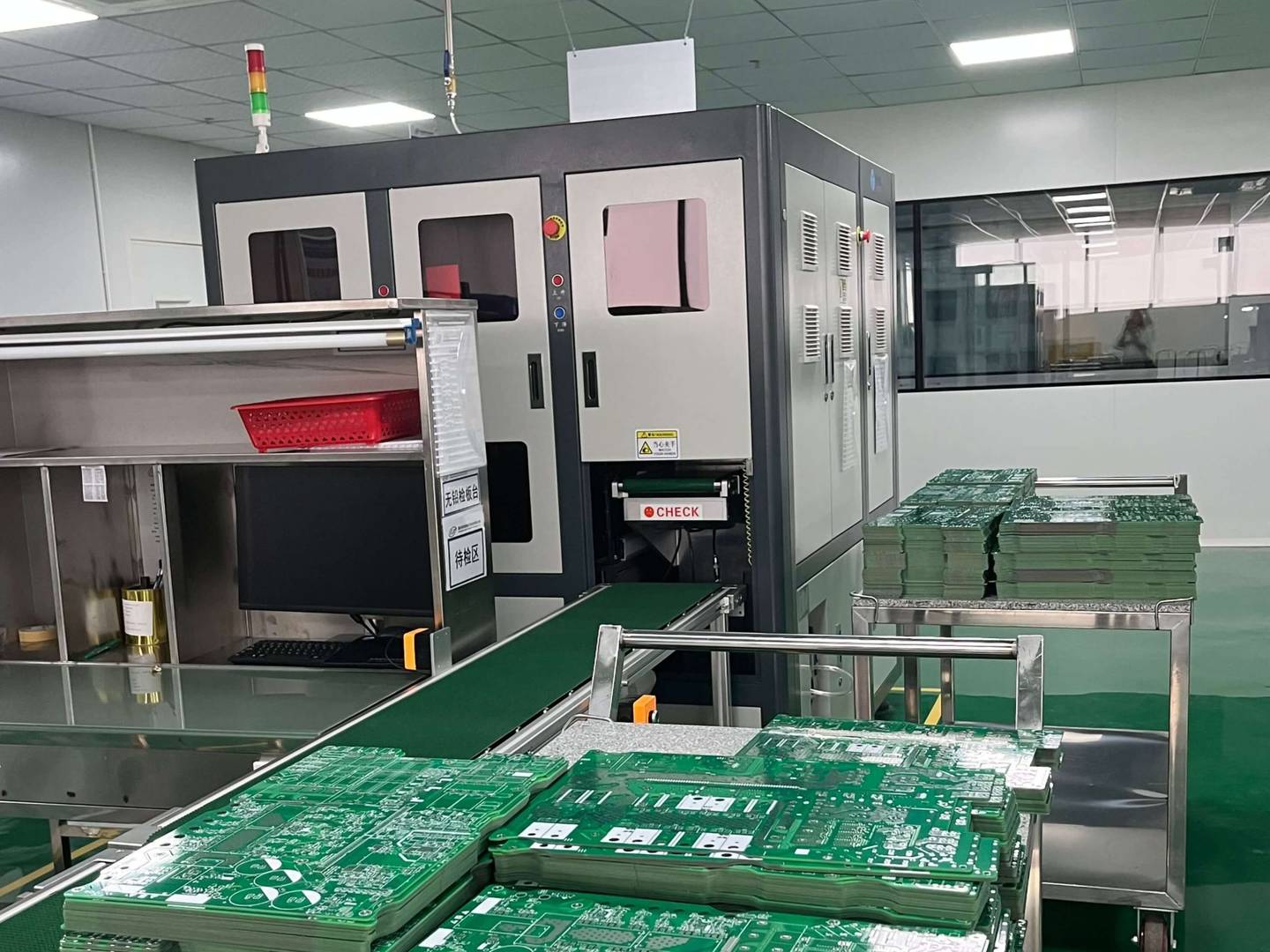
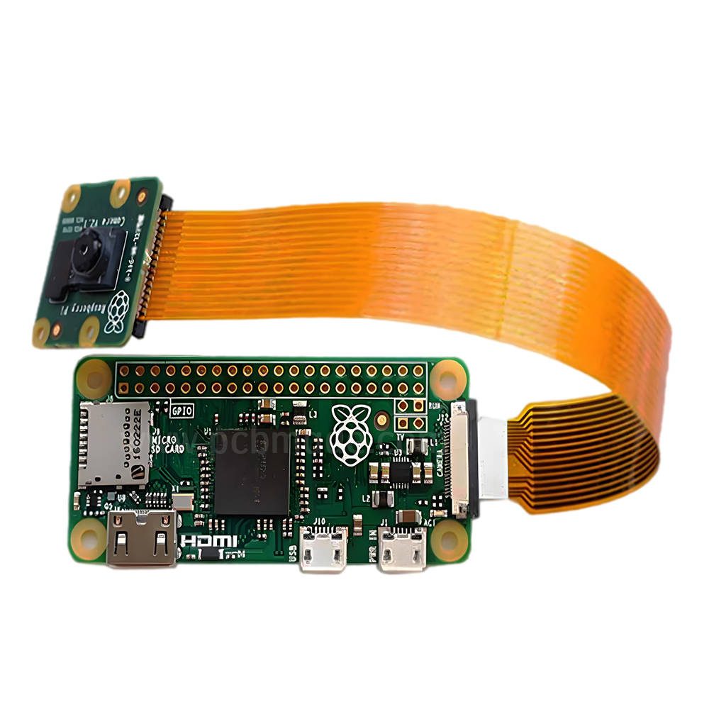

For the field of electronic design, microcontroller PCB board electronic design is a mysterious and innovative black technology. A microcontroller is a microcomputer system that integrates a central processing unit (CPU), memory, and input/output (I/O) interfaces. The electronic design of its PCB board is the key to building a microcontroller system.
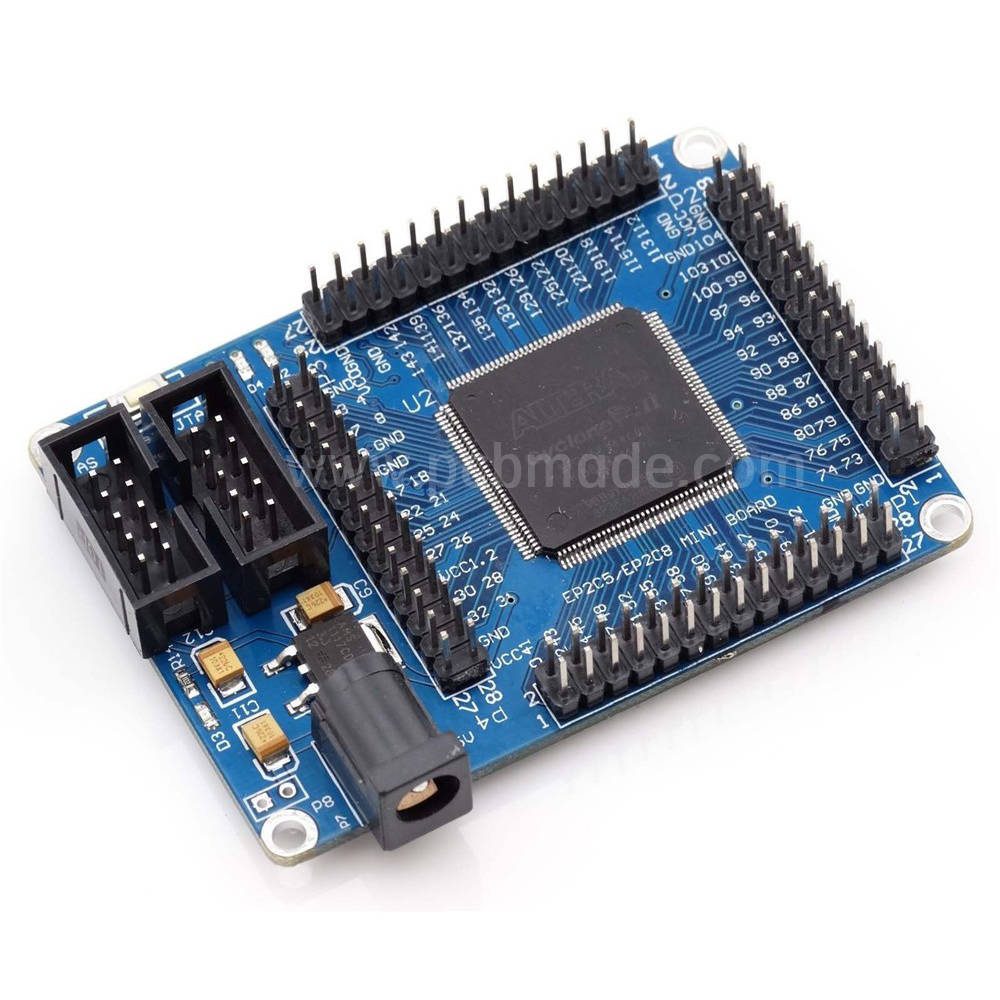
1、 Schematic design
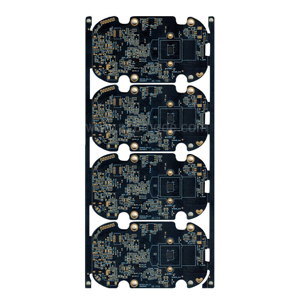
Schematic design is the first step in the electronic design of a microcontroller PCB board. It is a drawing that displays the connection relationship between circuit components and electronic components. Through schematic design, engineers can clearly understand the composition of circuits and the transmission paths of signals.
2、 Circuit layout design
Circuit layout design is the process of arranging and arranging electronic components in a reasonable position on a PCB board. Reasonable circuit layout design can minimize electromagnetic interference and signal crosstalk to the greatest extent possible. In this process, engineers need to fully consider factors such as the path length of signal transmission, the position of signal pins, and the physical distance between electronic components.
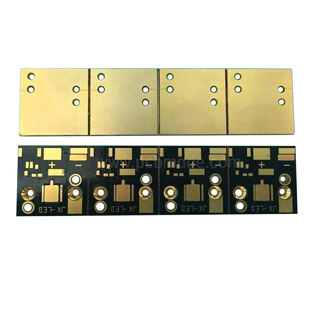
3、 Pad design
Pad design refers to providing soldering positions and connections for electronic components. Fine solder pad design can improve the stability and reliability of soldering. In the electronic design of microcontroller PCB boards, the size, shape, and arrangement of solder pads can also affect the performance of the circuit.
4、 Power cord design
Power cord design is the process of providing the necessary power to electronic components. In the electronic design of microcontroller PCB boards, a stable power supply is crucial to ensure the normal operation of the system. Engineers need to consider factors such as the length, width, and spacing of power lines to ensure the stability and reliability of the power supply.
5、 Signal line design
Signal line design is the process of transmitting signals between various electronic components. Reasonable signal line design can effectively reduce signal interference and power consumption in the electronic design of microcontroller PCB boards. Engineers will determine the length, direction, and width of signal lines based on their characteristics and transmission requirements.
6、 Grounding and shielding design
Ground wires are arranged to ensure the grounding of circuits and the stability of signals, while shielding is used to avoid the influence of electromagnetic interference. Reasonable grounding and shielding design can improve the performance and anti-interference ability of the system in the electronic design of microcontroller PCB boards.
By revealing these black technologies in the electronic design of microcontroller PCB boards, we can gain a deeper understanding of the innovation and challenges in the field of electronic design. I hope this article can provide some inspiration for readers interested in this field and inspire more exploration and research.