GND is an important component in electronic circuit boards, which provides a current return path and eliminates interference. The correct design of circuit board GND is the key to ensuring the normal operation of the circuit.
一、 The significance of circuit board GND
Circuit board GND, also known as ground wire, refers to the current return path of an electronic circuit board. It is connected to the negative pole of the power supply in the circuit, serving to connect electronic components, conductive wires, and external devices. Through the circuit board GND, the current of electronic components can smoothly flow back, ensuring the normal operation of the circuit. At the same time, the circuit board GND can also play a role in shielding electromagnetic interference.

二、 Design principles for circuit board GND
1. Single point grounding principle
In the process of circuit board design, the principle of single point grounding should be followed as much as possible. Connect all ground wires to a common location to avoid the formation of multiple grounding points, in order to reduce interference and asymmetry of the return path.
2. Layout of GND plane
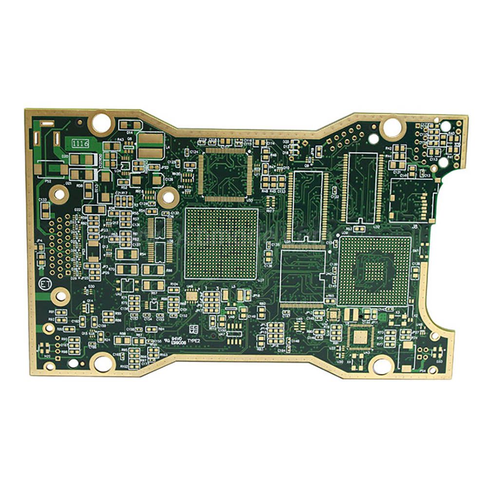
In PCB design, it is advisable to plan an independent plane for the layout of GND as much as possible. This plane can serve as a path for current backflow and act as a shield against electromagnetic interference. At the same time, in order to avoid interference, the GND plane should be kept at a certain distance from the signal and power lines as much as possible.
3. Layered wiring
For large and complex circuit boards, it is recommended to design GND using layered wiring. GND can be divided into multiple levels and wired according to different circuit parts, thereby reducing the asymmetry of the return path and better shielding interference.
4. Separation of GND and signal lines
In circuit board design, GND and signal lines should be separated as much as possible to avoid mutual interference caused by sharing the same layer plane. GND can be separated from signal lines by dividing regions on the GND plane and using layered wiring.
三、 Precautions for GND of circuit board
1. Avoid excessive GND return path
In circuit board design, the length of the GND return path should be minimized as much as possible. An excessively long reflux path can increase the impedance of the reflux current, affecting the stability of the circuit. Therefore, in the design process, the layout of the grounding wire should be reasonably planned to make the return path as short as possible.
2. Prevent GND backflow interference
The current in the GND return path may cause electromagnetic interference, affecting the normal operation of the circuit. To eliminate this interference, filtering inductors and capacitors can be added to the return path to provide isolation and filtering.
3. Crossing of GND and signal lines
During the wiring process of the circuit board, cross crossing between GND and signal lines should be avoided. Due to the signal carried by the signal line and the shielding effect of GND, their crossing can cause mutual interference of signals. Therefore, during the wiring process, the paths of GND and signal lines should be planned reasonably to minimize the possibility of crossing.


