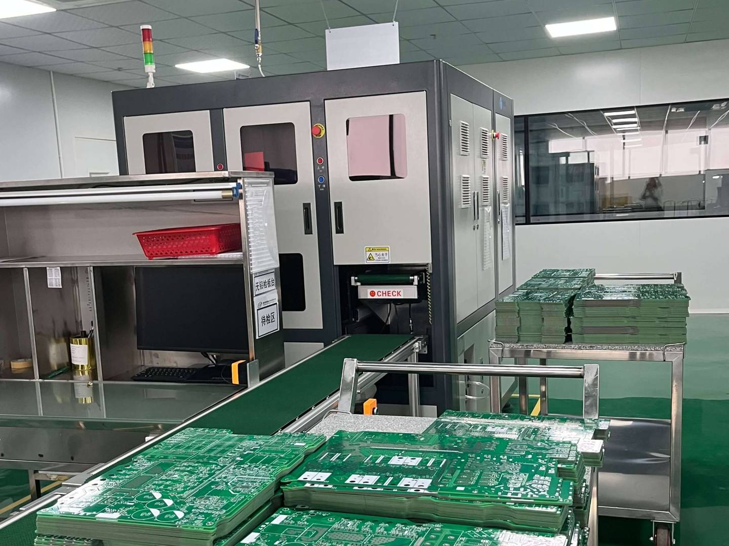
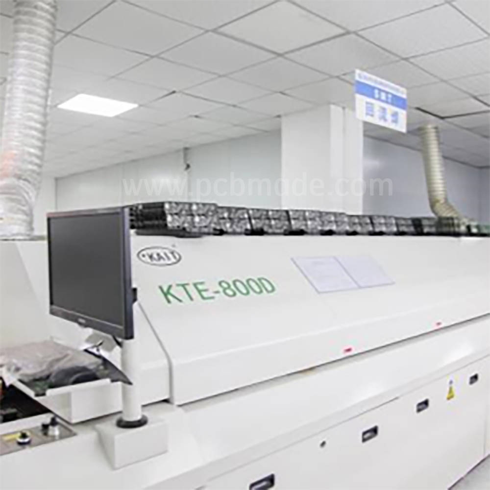

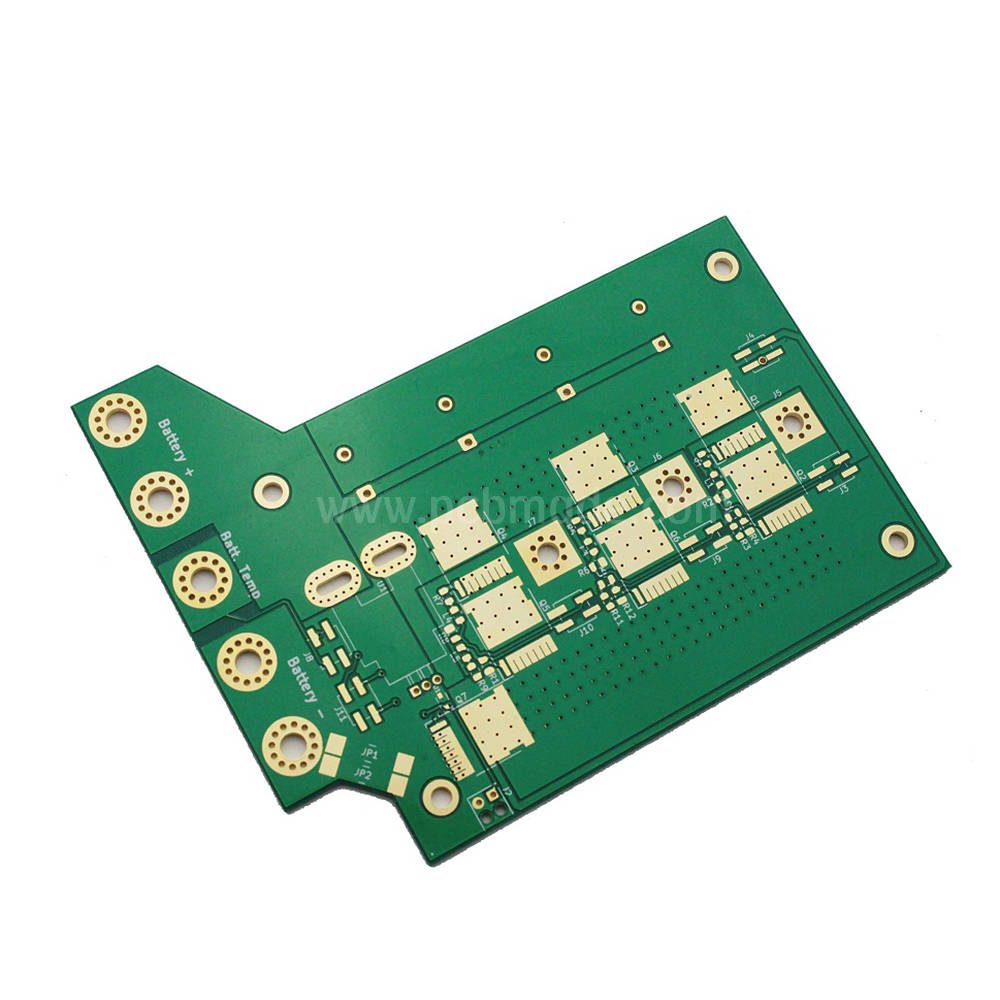
The optimization of motor drive PCB design scheme is crucial for the stability and performance of motor operation. This article will introduce how to optimize the motor drive PCB design scheme from three aspects: layout optimization, signal integrity, and power consumption control.
Layout optimization:
Good layout design can reduce electromagnetic interference and improve circuit stability.
Firstly, sufficient distance should be maintained between the motor drive circuit and the logic/control circuit to reduce mutual interference.
Secondly, try to minimize the loop area by placing the input and output terminals close to one side to prevent interference caused by loop induction. In addition, in PCB layout, attention should be paid to the design of the ground wire, and the return path of the ground wire should be shortened as much as possible to reduce inductance.
Finally, it is important to separate the analog and digital parts and arrange them separately in different areas.
Signal integrity:
In the design of motor drive PCB, signal integrity is a key issue. To ensure the stability and reliability of signal transmission, the following points can be considered.
Firstly, for long-distance transmission, it is important to pay attention to impedance matching and select appropriate transmission lines and differential signal transmission to reduce reflections and crosstalk on the transmission lines.
Secondly, for high-speed signal transmission, attention should be paid to the routing and routing rules of signal lines to avoid signal integrity issues caused by excessively long signal return paths.
In addition, using appropriate terminal resistors and shielding designs can effectively reduce signal interference and noise.
Power consumption control:
Power consumption control in motor driven PCB design is crucial for improving equipment efficiency and extending battery life. To achieve power consumption control, multiple approaches can be taken.
Firstly, choose low-power components such as MOSFETs and power management chips.
Secondly, optimize the power supply layout, reduce the length of the power consumption circuit, lower the resistance of the wires, and improve the efficiency of the power supply.
In addition, the power management module should be designed reasonably to achieve dynamic power consumption management of the motor, and the power supply and working mode of the motor should be adjusted according to actual needs.
In summary, to optimize the motor drive PCB design scheme, it is necessary to start from layout optimization, signal integrity, and power consumption control. Good layout design can reduce electromagnetic interference and improve circuit stability; The guarantee of signal integrity can improve the reliability of signal transmission; Power consumption control is crucial for improving device efficiency and extending battery life.