
In the precise world of modern electronic devices, every tiny component plays a crucial role. Among them, the quality and reliability of PCB printed circuit board, as the supporting skeleton and interconnect medium of electronic components, directly affect the performance and lifespan of the entire product. Therefore, professional circuit board manufacturers have strict requirements for PCB inspection and acceptance standards.
Basic understanding of PCB
PCB is a circuit board that uses electronic printing technology to pre design and manufacture conductive paths on an insulating substrate. It can provide mechanical support for various electronic components and achieve electrical connections between components. With the advancement of technology, PCBs have evolved from single-layer to complex types such as double-layer, multi-layer, and even high-density interconnect (HDI), and are widely used in consumer electronics, communication, medical, aerospace, and other fields.
The Importance of PCB Inspection
The quality of PCB is directly related to the functional implementation, stability, and service life of electronic products. Any minor defect, such as short circuit, open circuit, poor porosity, copper foil peeling, or residual contaminants, can lead to product failure. Therefore, a strict inspection process is a key step in ensuring PCB quality.
The main stages of PCB inspection
Raw material inspection: Before production, all raw materials, including copper-clad laminates, copper foils, solder mask inks, etc., must undergo strict inspection to ensure that the materials meet the specifications and are free of impurities and damage.
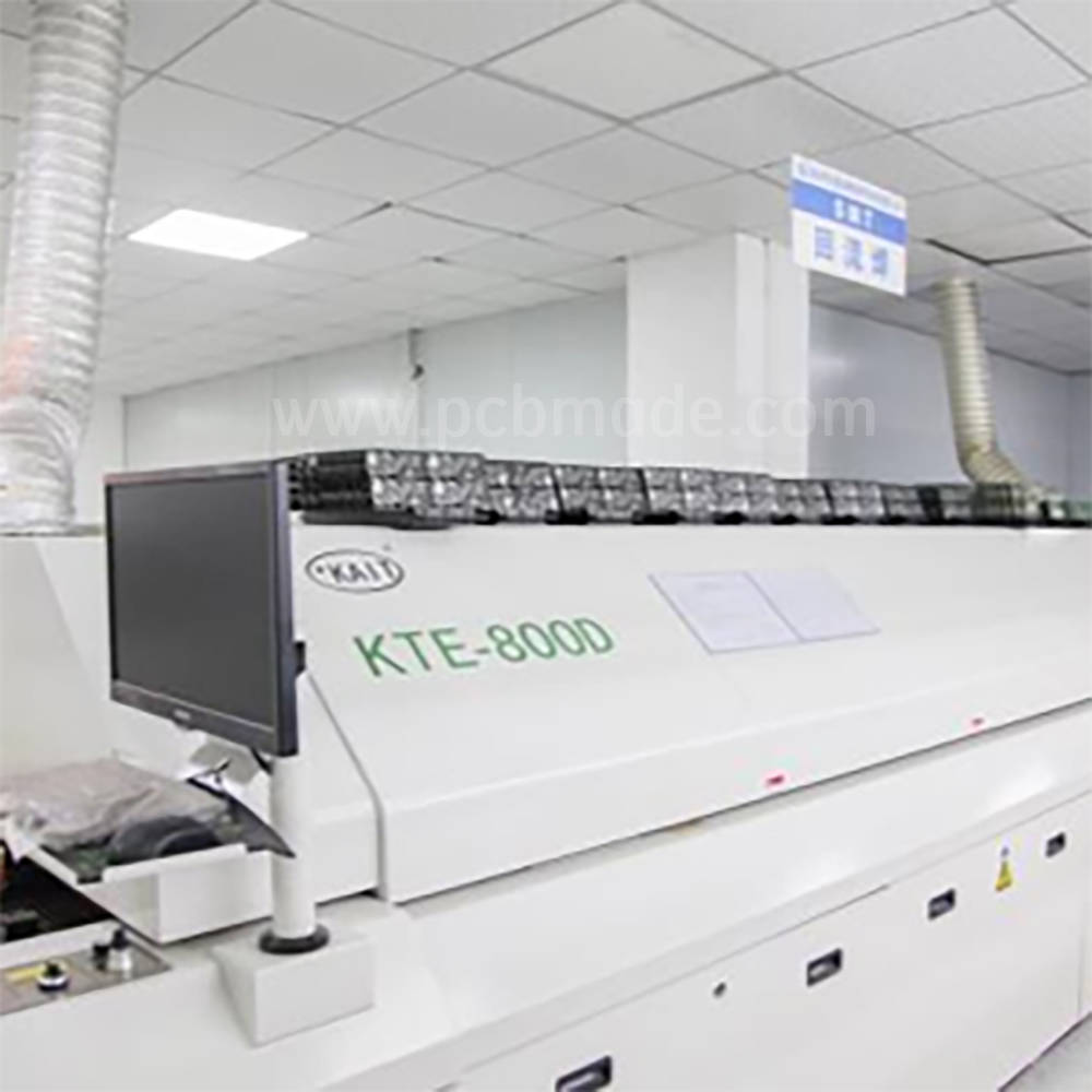
Process inspection:
Inner layer production inspection: check the accuracy of the etched circuit, copper plating thickness, etc.
Laminated inspection: In the production of multi-layer boards, it is necessary to inspect the alignment between layers and the condition of bubbles.
Drilling inspection: Confirm the accuracy of the hole position and the smoothness of the hole wall.
Surface treatment inspection: After gold plating, tin plating, OSP treatment, it is necessary to check the surface uniformity and adhesion.
Finished product inspection:
Appearance inspection: Check for scratches, deformation, and contamination.
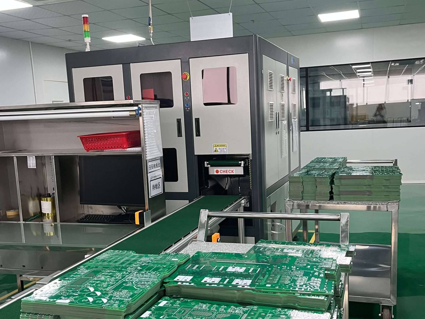
Electrical testing: Use methods such as flying pin testing, AOI (automatic optical inspection), AXI (automatic X-ray inspection), etc. to detect issues such as conductivity, insulation resistance, short circuits, or open circuits.
Functional testing: Some high-end products will undergo functional testing that simulates actual working environments to ensure the performance of the circuit board in applications.
Acceptance Criteria
The acceptance standards of professional circuit board manufacturers are usually based on internationally recognized standards, such as IPC-A-600 (Acceptance Conditions for Rigid Printed Boards), IPC-A-610 (Acceptability Standards for Electronic Components), etc. These standards specify various quality requirements from materials, manufacturing processes to final products, including but not limited to:
Dimensional tolerance
Consistency of line width/spacing
Aperture accuracy
Surface coating quality
Electrical performance indicators
Only when the PCB passes all the inspection steps mentioned above and each indicator meets or exceeds the specified acceptance standards, can it be considered a qualified product and delivered to the customer.
The importance of quality control for PCB, as the core component of electronic products, is self-evident. Professional circuit board manufacturers ensure that every PCB meets or even exceeds industry standards through a series of rigorous inspection processes and high standard acceptance criteria, providing customers with reliable and efficient electronic solutions. With the continuous advancement of technology, future PCB inspection technology will also become more intelligent and efficient, providing strong support for the sustainable development of the electronics industry.