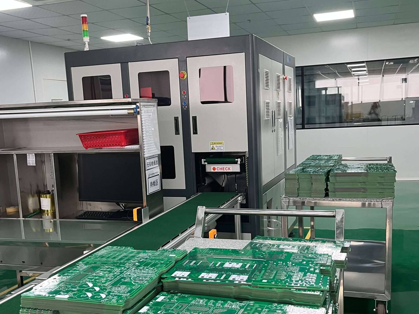

In the microscopic world of electronic devices, PCB (Printed Circuit Board) plays the role of a “neural network” that connects and supports various electronic components. As the core component of electronic devices, the quality of PCB directly affects the performance and lifespan of the product. Among them, the surface treatment process of PCB is an important link that determines its electrical performance and reliability.
1. Tin plating (HASL, Hot Air Solder Leveling)
Tin plating, especially hot air leveling (HASL) process, is one of the most traditional and cost-effective PCB surface treatment methods. This process involves immersing the PCB in melted solder, followed by using hot air to remove excess solder, thereby forming a uniform tin coating on the copper surface. This processing method can provide good solderability and is suitable for most general electronic products. However, with the increasing demand for finer circuits and lead-free requirements, the use of HASL has decreased, especially on high-density interconnect (HDI) boards.
2. Electroless Nickel Immersion Gold (ENIG)
Chemical nickel gold plating is a more advanced and widely used surface treatment technology, particularly suitable for thin line spacing and high-density PCBs. This process first deposits a layer of nickel on the copper surface, and then deposits a thin layer of gold. The gold layer serves as a protective layer to prevent oxidation of the nickel layer and provide long-term welding reliability and good weldability. ENIG technology has become the preferred surface treatment method for many high-end electronic products due to its excellent corrosion resistance and long-term stability.
3. Organic Solderability Preservative (OSP)
Organic solder paste (OSP) treatment is an environmentally friendly and cost-effective surface treatment technology, particularly suitable for PCBs with low to medium complexity. This process involves coating a thin layer of organic compound on the exposed copper surface to protect it from oxidation while maintaining good weldability. OSP processed PCBs have lower surface contours and are suitable for high-frequency signal transmission, but their storage conditions and service life are relatively strict, making them unsuitable for long-term storage or harsh environmental applications.
4. Immersion Silver plating
Electroplated silver, also known as immersion silver, is a surface treatment technique that deposits a layer of silver on a copper surface through chemical reactions. The silver layer not only provides excellent conductivity and solderability, but also has good corrosion resistance. Compared to gold plating, silver immersion has a lower cost, but the silver layer is thinner and prone to oxidation, especially in high temperature and humid environments, making it more suitable for cost sensitive and short-lived products. The silver immersion process has a wide range of applications in fields such as communication, consumer electronics, and automotive electronics.
In summary, choosing the appropriate PCB surface treatment process should be determined based on the product’s requirements, cost budget, environmental requirements, and expected service life. Each process has its unique advantages and applicable scenarios, and understanding these basic knowledge can help designers and manufacturers make more informed choices, thereby ensuring the quality and reliability of electronic products. With the continuous advancement of technology, there may be more innovative surface treatment technologies in the future, bringing more possibilities to the electronics industry.