
In the world of electronic devices, printed circuit boards (PCBs) are essential core components that carry the construction and operation of complex circuits. However, PCBs may experience warping and deformation during the production process, which seriously affects their assembly performance and overall equipment stability. To this end, professional PCB manufacturers have taken a series of scientifically rigorous preventive measures to ensure product quality and meet customers’ demands for high precision and high performance.
1、 Optimize material selection and storage
Selected substrate: The source of PCB warping often begins with the selected substrate. High quality PCB manufacturers will choose copper-clad laminates with low CTE (coefficient of thermal expansion) and stable mechanical properties as raw materials to reduce the risk of deformation caused by temperature changes.
Strictly control humidity: During storage and use, humidity has a significant impact on the flatness of the substrate. Manufacturers will set up a constant temperature and humidity warehouse to ensure that the substrate is within a suitable humidity range (usually 40% -60% RH), preventing warping caused by moisture absorption or evaporation.
2、 Accurate design and process layout
Balanced layer design: During the multi-layer PCB design phase, engineers will plan the routing, power and ground distribution, and embedded component positions of each layer reasonably, striving to achieve uniform stress distribution between layers and avoid warping caused by local stress concentration.
Control the uniformity of copper thickness: Uneven copper foil thickness is also one of the factors that cause warping. By precisely controlling the etching process, the consistency of copper thickness in various parts can be ensured, which helps to reduce warping caused by uneven weight distribution.
Pre set anti warping grooves: For large or high-density PCBs, designers will pre set anti warping grooves (such as serpentine grooves, stress relief grooves, etc.) on the board edge or inside, using groove structures to absorb and disperse stress, preventing overall warping.
3、 Fine process control
Optimization of hot pressing process: During the multi-layer board pressing process, the manufacturer will precisely control the pressing temperature, pressure, and time to ensure that the bonding between each layer is firm and the stress is fully released. At the same time, advanced pressing strategies such as gradual heating and stepped pressure are adopted to reduce the risk of warping caused by one-time high temperature and high pressure.
Precision drilling and decontamination: Drilling is a critical step in PCB manufacturing, and deviations in drilling, rough hole walls, or incomplete decontamination can all lead to stress concentration. The manufacturer will use high-precision CNC drilling machines, combined with high-quality drilling needles and anti drilling technology, to ensure hole quality and reduce the risk of warping.
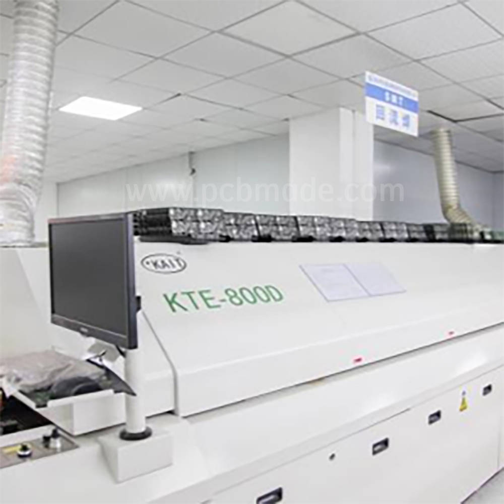
Strict control of reflow soldering parameters: During SMT surface mount soldering, excessive reflow temperature or uneven heating may lead to increased thermal stress on the PCB. Manufacturers will refine the reflow soldering curve based on the characteristics of the board and the requirements of the components, ensuring a gentle and uniform soldering process and reducing the risk of warping.
4、 Strict quality inspection and control
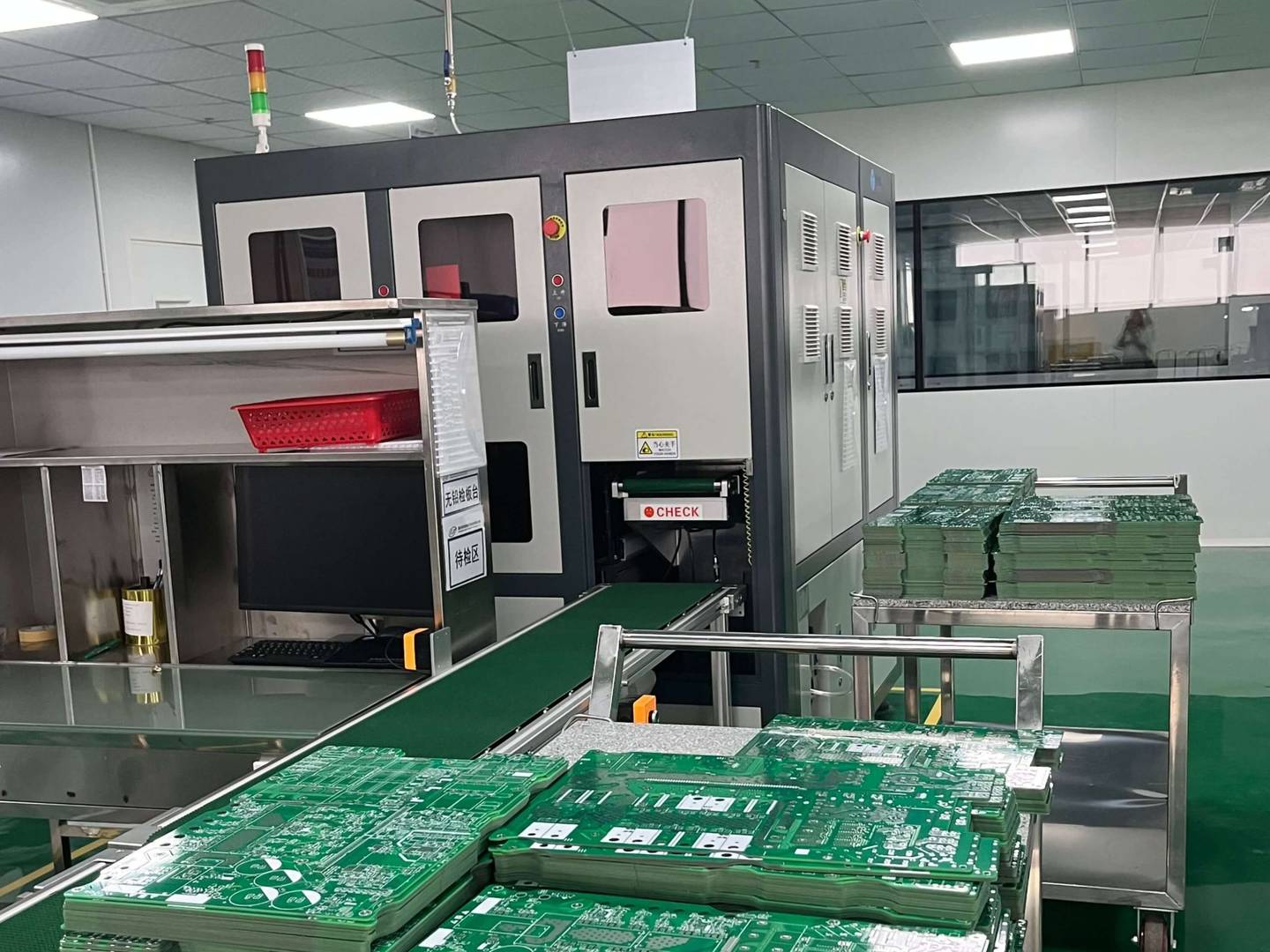
Online warpage monitoring: In the production process, manufacturers will use automatic optical inspection (AOI), X-RAY and other equipment to monitor the flatness of PCBs in real time. Once warpage exceeds the limit, process parameters will be adjusted or rework will be carried out immediately.
Finished product warpage detection: The finished PCB needs to undergo strict warpage detection, usually measured using a dedicated warpage testing machine to ensure that the product meets industry standards or customer specific requirements.
In summary, PCB manufacturers have developed a comprehensive and multi-level system for preventing warping and deformation through carefully selected materials, precise design, fine process control, and strict quality inspection. This series of professional measures not only ensures the high-quality output of products, but also reflects the manufacturer’s deep understanding of process technology and high attention to customer needs, providing a solid hardware foundation for the stable operation of electronic devices.