Ensuring quality and performance is crucial in the design and manufacturing process of PCB printed circuit boards, the core of electronic products. Among them, the phenomenon of “copper leakage” is a common problem that may occur in PCB production, which directly affects the electrical characteristics, reliability, and appearance quality of the circuit board.
一、 Understanding PCB board “copper leakage”
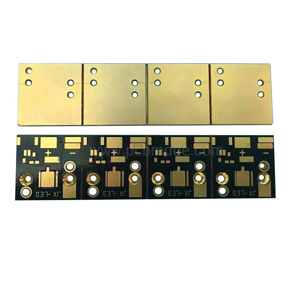
Copper leakage “refers to the phenomenon in the PCB manufacturing process where exposed copper foil (such as wires, pads, etc.) that should have been covered by a solder mask is not completely covered due to design, processing, or material factors, and is exposed to the outside. This’ copper leakage ‘may occur at any position on the board surface, including but not limited to via holes, wire edges, and around solder pads.
The hazards of copper leakage mainly manifest in the following aspects:
Electrical hazards: Uncovered copper foil may pose a risk of short circuit, especially in humid environments or in contact with foreign objects, which may cause circuit abnormalities or even equipment damage.
Welding problem: Excessive exposed copper surface will increase the consumption of solder paste during welding, affecting the welding quality and potentially leading to welding defects such as virtual soldering and bridging.
Reduced reliability: The exposed copper surface is prone to oxidation, reducing the corrosion resistance of the circuit board and affecting its long-term stability.
Impaired aesthetics: From an appearance perspective, “copper leakage” can make the PCB appear irregular and affect the product image.
二、 How to cover “copper leakage”
There are several common methods to address the issue of copper leakage, including:
1. Optimize the design and process of solder mask layer
This is the most direct and fundamental solution. In the PCB design phase, it is important to ensure that the solder mask design is precise and error free to avoid “copper leakage” caused by design negligence. In the production process, the coating process of the solder mask should be strictly controlled to ensure that it evenly and completely covers the copper surface that needs to be protected.
2. Use touch up paint or repair glue
For PCBs that have already experienced “copper leakage”, specialized solder mask or repair glue can be used for local repair. This type of product can cure at room temperature, forming an insulating protective layer that effectively covers the exposed copper surface.
3. Selective electroplating
In certain specific cases, a selective electroplating process can be used to deposit a layer of other metals (such as nickel, gold, etc.) at the “copper leakage” site, which not only provides coverage protection but also enhances local corrosion resistance.
三、 Can PCB board copper leakage be covered with tin?
The answer to the question of whether “leaking copper” can be covered by adding tin is: it can be done under specific conditions, but it is not the best solution and requires careful operation.
Firstly, adding tin can indeed cover the “leakage copper” to a certain extent, preventing it from coming into direct contact with the environment and reducing the risk of short circuits and oxidation. However, this method has the following limitations:
1.Cost increase: Additional solder paste consumption will increase production costs and may require manual intervention, affecting production efficiency.
2.Welding problem: Excessive solder paste accumulation may cause uneven heat distribution during welding, leading to welding quality issues.
3.Reliability uncertainty: Solder paste itself is not an ideal insulation material, and there may be a risk of insulation failure after prolonged use. In addition, solder paste is prone to oxidation, sulfurization and other reactions in high temperature and humid environments, which affect its coverage effect and circuit stability.
Therefore, although adding tin can be a temporary measure to deal with “copper leakage” in emergency situations, in the long run, optimizing the design and process of the solder mask layer, or using professional methods such as repainting, repairing glue, and selective electroplating, is more reliable and effective.
In summary, the issue of “copper leakage” in PCB boards cannot be ignored and should be effectively covered through scientific and reasonable means. Although adding tin can to some extent mask “copper leakage”, it is not an ideal choice due to limitations in cost, soldering, and reliability. Prioritizing the optimization of solder mask design and process, or using professional repair materials and processes, is the wise move to ensure PCB quality and performance.


