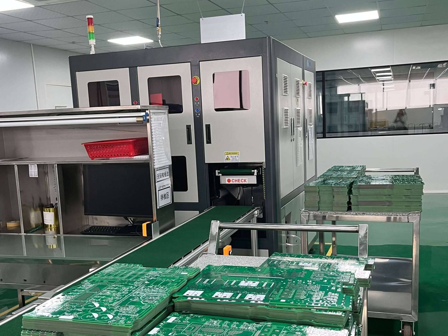

With the rapid development of electronic technology, high-speed PCBs (printed circuit boards) are becoming increasingly widely used in modern electronic products, from smartphones to high-performance computers, everywhere. The design of high-speed PCB not only concerns the performance stability of the product, but also directly affects key indicators such as signal integrity, power integrity, and electromagnetic compatibility. Therefore, following a rigorous set of design rules is crucial for ensuring the efficient operation of high-speed PCBs.
1. Signal Integrity (SI) Management
Application of transmission line theory: In high-speed design, signal lines are considered as transmission lines, and characteristic impedance matching needs to be considered. Ensuring that the characteristic impedance (usually 50 Ω or 100 Ω) of all signal lines remains consistent can reduce reflection and crosstalk.
Signal line length matching: For clock signals and differential pair signals, line length matching should be maintained as much as possible to reduce signal distortion caused by time delay differences.
Terminal matching: Using appropriate terminal resistors (such as series terminals, parallel terminals, or AC terminals) can effectively absorb signal reflections and ensure signal quality.
2. Power Integrity (PI) and Decoupling
Power plane design: Using large areas of power and ground planes not only provides a good power return path, but also enhances EMC (electromagnetic compatibility).
Decoupling capacitor arrangement: Place multiple decoupling capacitors with different capacitance values (such as 100nF, 1 μ F, 10 μ F) near the key IC power pins to filter out noise in different frequency ranges.
3. Stacking design and wiring strategy
Stacking structure: Reasonably planning the stacking structure of PCB to ensure sufficient power/ground plane layers can help reduce crosstalk and improve signal quality.
Wiring spacing: Reduce the distance between high-speed signal lines and other wiring to minimize crosstalk. It is generally recommended that the distance between high-speed signal lines and adjacent lines be at least 3 times the line width.
Avoid right angle routing: Use 45 degree or circular arc turns to reduce high-frequency signal radiation and impedance discontinuity.
4. Electromagnetic compatibility (EMC) considerations
Shielding and isolation: Sensitive circuits or high-frequency components are isolated using shielding covers or ground wires to prevent external interference and internal signal leakage.
Return path optimization: Ensure that all signal lines have clear and continuous return paths, usually the nearest ground plane, to minimize loop area and reduce radiation.
5. Thermal management
Heat dissipation design: For high power components, large-area copper foil is used as the heat sink, and air duct design is considered to improve the system’s heat dissipation efficiency.
High speed PCB design is a complex and intricate task that requires designers not only to be proficient in circuit knowledge, but also to have a deep understanding of materials and electromagnetic theory. The above rules are only the tip of the iceberg, and in actual design, flexible adjustments need to be made according to specific applications and standards. Continuously learning the latest design techniques and tools, combined with simulation software to verify the design, is the key to improving the success rate of high-speed PCB design. With the continuous advancement of technology, the challenges and opportunities of high-speed PCB design coexist, and continuous exploration and practice are compulsory courses for every electronic engineer.