
In the world of modern electronic technology, printed circuit boards (PCBs) are the core components of various electronic devices, carrying the electrical connections between electronic components. However, in the PCB production process, a common quality issue – “PCB hole breakage” – not only affects product quality, but may even lead to the failure of the entire circuit board.
What is PCB hole breakage?
PCB hole breakage, as the name suggests, refers to the phenomenon of conductive or non-conductive through holes (such as through holes used to fix components) on a PCB board breaking, fracturing, or damaging the hole walls during the manufacturing process. This may be due to excessive mechanical stress during the drilling process, or improper handling of subsequent processes such as chemical copper deposition and electroplating. The problem of hole breakage can affect the integrity and reliability of the circuit, and in severe cases may cause signal transmission interruption or component installation failure.
Detection method for PCB hole breakage
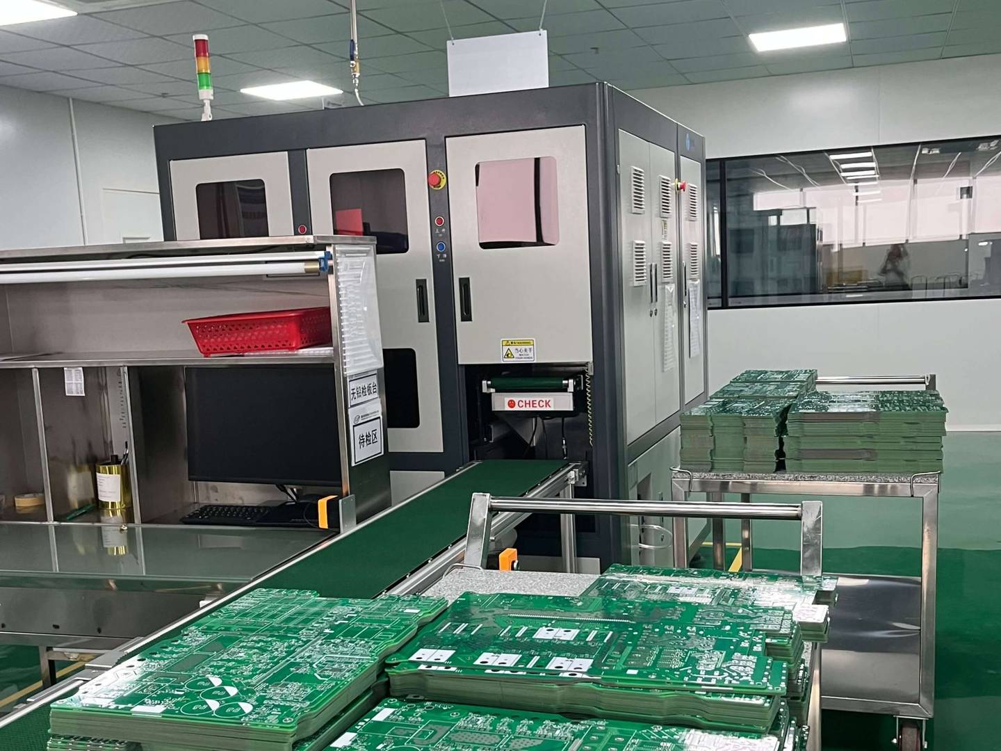
Optical inspection: Using high-precision optical inspection equipment and image recognition technology, the holes on the PCB board are scanned in all directions to detect and locate the location of the holes. This method is intuitive, efficient, and suitable for large-scale automated testing.
Electrical measurement method: By conducting current testing on the metalized layer inside the hole, it is determined whether there is an open circuit in the hole based on the current passing through, thereby detecting the problem of hole breakage.
X-ray inspection: For multi-layer boards and buried hole boards, X-ray perspective inspection technology can be used to determine whether there are holes or other defects by observing the internal structure of the holes.
Ultrasonic testing: By utilizing the characteristic of the difference in propagation speed of ultrasonic waves in different media, the integrity of the hole wall can be detected, which has a good detection effect on hole breakage problems that are difficult to directly observe with the naked eye or optical equipment.
Exploration and Solution Strategies for PCB Hole Breaks
To prevent and solve the problem of PCB hole breakage, it is necessary to start from multiple aspects such as design, manufacturing process, and material selection:
Design phase: Reasonably design the aperture size and spacing to avoid increasing the risk of hole breakage due to excessively small aperture and thin hole walls; Optimize wiring layout to reduce areas of high stress concentration.
Manufacturing process: Optimize drilling parameters, control drilling force and speed; Improve the process flow of chemical copper deposition, electroplating, etc., to ensure uniform coating and moderate thickness of the hole wall.
Material selection: Select high-quality PCB substrates to ensure they have sufficient mechanical strength and corrosion resistance, reducing the possibility of hole breakage.
In summary, PCB hole breakage is an important quality control point in the PCB production process. Through scientific testing methods and rigorous production process improvements, we can effectively prevent and solve this problem, thereby improving the overall quality and service life of PCB circuit boards and providing strong guarantees for the stable operation of electronic products